India’s Next DLI Phase Targets 70–75% “Domestic Chip Coverage” by 2029
Published: 2.5.2026
Key takeaways
- India is positioning DLI’s next phase as a scale-up effort targeting 50 fabless companies and focusing on six chip categories (logic/compute, RF, networking, power management, sensors, memory).
- The roadmap ties domestic tape-outs to SCL Mohali (180nm) and points to the upcoming Dholera fab as the next rung (often referenced as supporting 28nm-class work).
- “Semicon 2.0” is being framed as an advanced-node ambition with a stated 3nm/2nm roadmap, though timelines differ across reporting.
- India plans on building a local base for high-volume, strategically important chips used across automotive/EV, industrial, power, telecom, and defense supply chains.
India’s government is outlining a 2029 goal to build the capability to design and manufacture chips that cover domestic application needs, as it scales its Design Linked Incentive (DLI) push, grows a fabless ecosystem, and connects tape-outs to a step-by-step manufacturing roadmap from mature nodes toward longer-horizon advanced-node ambitions.
Union IT Minister Ashwini Vaishnaw said India aims to build capability to design and manufacture chips used in “70–75%” of domestic applications by 2029.
This reframing is central to the next phase of the Design Linked Incentive program. The emphasis is moving from “proof of activity” toward commercially relevant outcomes, more product-bound designs, more repeatable tape-out cycles, and tighter integration with manufacturing readiness.
1) Aiming for 50 Fabless Companies
Government messaging around the next phase includes a target of enabling at least 50 fabless semiconductor companies to increase design throughput & productization, and to strengthen the ecosystem links required to ship silicon at scale.
That scale-up implies:
- more tape-outs that go beyond demos,
- more productization (qualification, reliability, manufacturing handoff),
- and stronger links to fabrication, packaging, testing, and demand aggregation.
2) Six chip domains as the “coverage strategy”
The six focus areas (logic/compute, RF, networking, power management, sensors, and memory) are framed as the building blocks behind a large share of electronic systems. These are the categories that recur across vehicles, factories, telecom networks, medical devices, consumer electronics, and defense platforms.
The Manufacturing Ladder
India’s roadmap is easiest to understand as a three-step ladder, with each rung serving a distinct role.
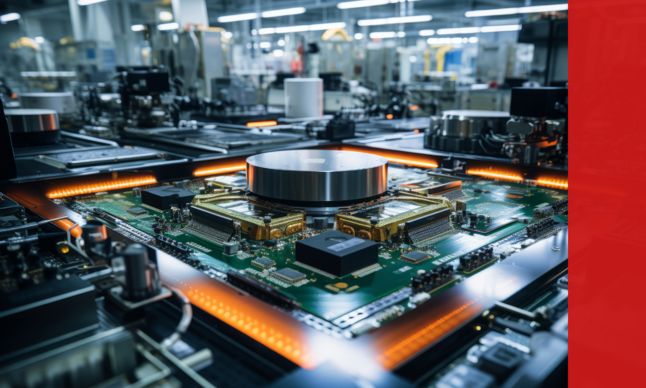
Step 1: SCL Mohali as the 180nm Anchor for Tape-outs
SCL Mohali is being positioned as a practical base for 180nm-class fabrication support, particularly for:
- academic and early-stage designs,
- government-aligned projects,
- “learn-by-building” validation cycles.
This facility is not intended to compete with commercial leading-edge foundries, but to provide a foundational manufacturing base for silicon enablement and skills development.
Step 2: Dholera as the Next Rung (up to 28nm)
The upcoming fab at Dholera is being discussed as a facility that can support substantially more advanced manufacturing than SCL often referenced as supporting down to 28nm-class capability.
That matters because 28nm (and nearby nodes) is still a workhorse tier for:
- industrial SoCs and controllers,
- networking silicon,
- automotive ECUs and gateway devices,
- power-adjacent control,
- secure/embedded systems.
For many of these markets, process maturity, qualification stability, and supply predictability are more critical than access to the most advanced nodes.
Step 3: “Semicon 2.0” and the 3nm/2nm destination
Alongside near-term execution, India has articulated a longer-horizon ambition, frequently described as “Semicon 2.0”, including a roadmap toward 3nm and 2nm manufacturing capabilities.
Timelines differ across public reporting, but the consistent signal is that India does not want to be structurally limited to mature nodes. At the same time, the 3nm/2nm roadmap should be read as a strategic destination requiring a much deeper ecosystem (equipment, materials, process know-how, packaging, yield discipline) than the near-term 28nm-class ramp.
Impact on Global Markets
Even if advanced-node manufacturing is a long path, the roadmap can still have near- and mid-term effects across key industries:
Automotive + EV
Local coverage of power management ICs, sensing, networking, and compute-adjacent silicon can reduce exposure to shortages especially for the long qualification cycles and platform lifetimes typical in automotive.
Industrial + automation
Industrial markets are packed with “not-leading-edge” chips that are absolutely mission-critical: controllers, connectivity, sensing, isolation, and power control. A stronger India design base could also increase demand for industrial-grade passives, protection, connectors, power modules, and ruggedized assemblies.
Power + energy
Grid modernization and renewables integration depend on power semis and controls, categories that map neatly to the “coverage” logic (power management, sensing, networking).
Aerospace + defense
The strategic value lies less in scale economics and more in trusted supply, qualification control, and long-term availability. Domestic silicon capability enhances assurance across sensitive and mission-critical systems.
Rather than positioning semiconductor self-reliance as a single jump to advanced nodes, India is laying out a sequenced pathway to expand design incentives, increase tape-out throughput, and connect those designs to domestic manufacturing rungs that match real-world application demand.
The clearest signal is not “India goes leading-edge overnight,” but India building a repeatable design-to-manufacturing pipeline starting where volume markets actually live, and aiming to climb over time.


