China Shrinks EUV: Hefei Lumiverse Unveils Desktop Light Source for 14nm Chips
Published: 11.27.2025
.png)
- Hefei Lumiverse has developed a desktop-sized EUV light source used in at least one 14nm production workflow.
- Although far less powerful than commercial EUV scanners, it enables inspection, R&D, and prototype-level processing.
- The device reflects a strategic milestone in China’s push to develop domestic EUV-class technologies.
- It does not replace ASML tools, but it expands access to EUV capabilities for labs, research lines, and smaller fabs.
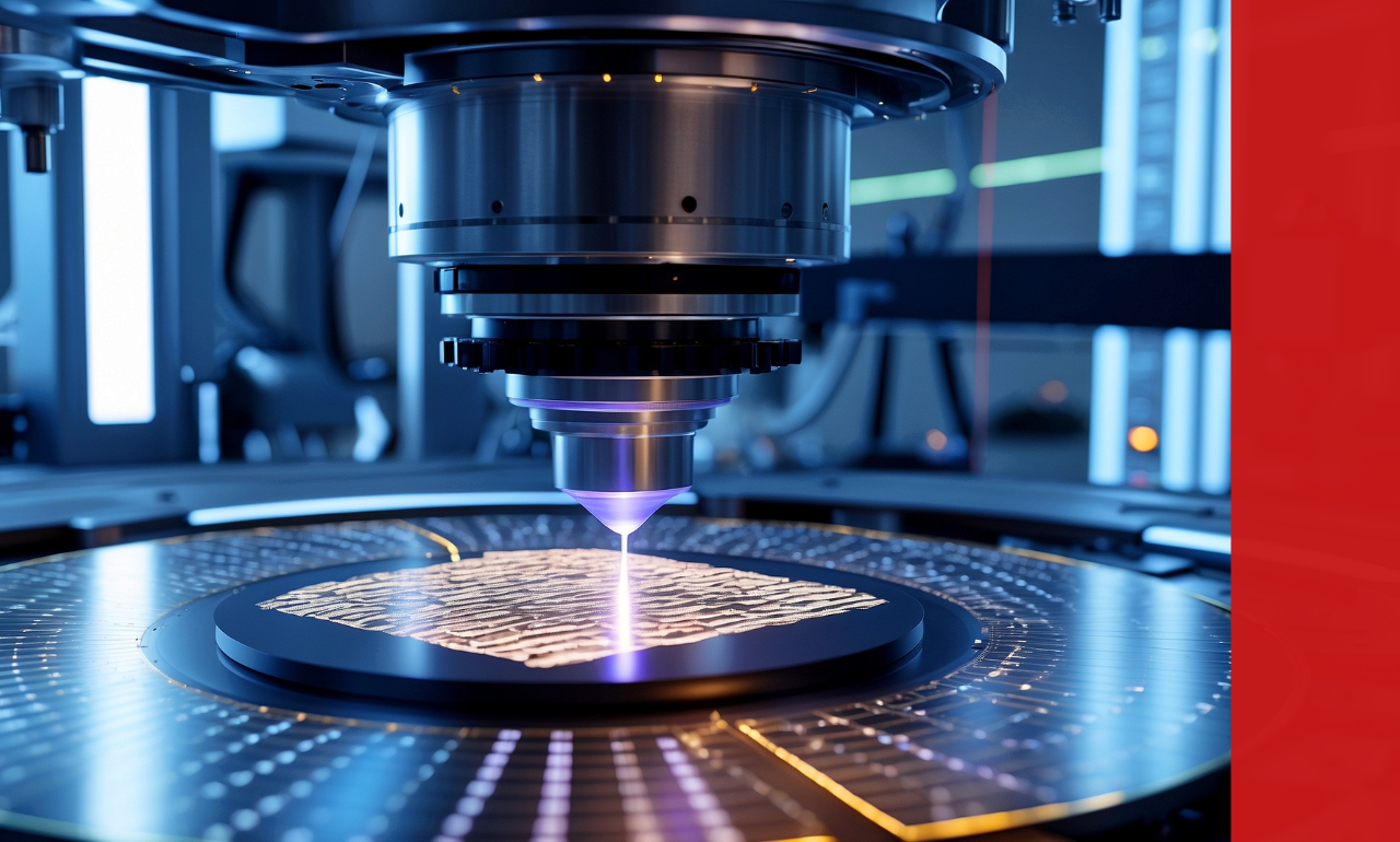
Hefei Lumiverse Technology has unveiled a desktop-scale extreme ultraviolet (EUV) light source a system small enough to sit on a table, yet reportedly already integrated by at least one industrial customer into a 14nm chip production flow.
Today’s chip industry is used to 12-meter-long EUV systems that weigh several tons and cost well over US$100 million. This new device is not positioned as a replacement for ASML’s high-volume scanners. For fabs, research labs, and regions that previously had no realistic way to work with EUV processes, this kind of compact source opens the door to new options in experimentation, inspection, and small-batch production.
A Different Kind of EUV Source
The device was introduced publicly at the UltrafastX conference in late October 2025. Instead of relying on the plasma-based architecture used in ASML scanners, Hefei Lumiverse built its light source using High Harmonic Generation using femtosecond laser pulses firing into inert gas to create high-order harmonics of light—essentially multiplying the frequency of the original laser until it reaches the EUV range.
Because of this design, the system is surprisingly flexible. Its output can be tuned from EUV wavelengths down to around 1 nm, up through soft X-rays. It’s a broad spectrum of capability, packaged in something closer to a lab instrument than a mega-tool.
This is not a complete lithography scanner. It’s a light source module, but one that dramatically lowers the physical footprint and cost of accessing EUV-class wavelengths. And that lower barrier is a big part of why this announcement drew global attention.
Why It Matters Even If It’s Not High-Volume Ready
Today, Hefei Lumiverse’s HHG source delivers around 1 microwatt at 13.5 nm. By comparison, the light sources inside ASML’s EUV systems reach more than 200 watts. That gap is not something incremental improvements can easily bridge.
Yet despite this huge disparity, the device plays a practical role. The public reporting indicates that a Chinese industrial customer incorporated the source into certain steps of a 14nm production flow. This doesn’t mean the device is printing full wafers. Instead, it likely supports mask inspection, materials research, line-edge roughness studies, or prototype exposures, all areas where the beam doesn’t need the power required for mass production.
This is part of what makes the story so interesting. It reflects a shift in how semiconductor ecosystems may evolve. Instead of only having massive, centralized facilities with billion-dollar tools, smaller fabs, labs, and research lines can begin accessing EUV-class processes for the first time, even if only for narrow tasks. That accessibility carries long-term strategic implications.
Why the 14nm Node Is Still Strategic
While global headlines focus on 3nm and 2nm race, the 14nm node continues to be one of the most widely used workhorse nodes across automotive, industrial automation, IoT, and consumer embedded systems for its stability and power-efficiency.-
Historically, EUV was supposed to debut at 14nm, but the technology wasn’t ready, and manufacturers such as TSMC and Samsung relied on multi-patterning with 193i lithography. The fact that a compact EUV/HHG source can now support any part of a 14nm process flow—even if limited—hints at a long-term shift: smaller-scale EUV tools might gradually find their way into mainstream manufacturing environments, at least for inspection and process control.
China, in particular, sees value in this. The ability to develop and deploy domestic EUV-class tools, even if they don’t rival ASML’s performance, supports the country’s broader push to localize critical semiconductor technology.
A Research Tool Today, a Strategic Asset Tomorrow
No one in the industry expects Hefei Lumiverse’s tabletop system to challenge ASML scanners. It is not a competitor; it is not intended to be one. But it represents something that has captured the semiconductor world’s attention: a proof-of-concept that EUV doesn’t have to stay massive, rare, and centralized.
For now, the company’s primary customers are universities, laboratories, and research institutions, not high-volume fabs. The system’s true value lies in enabling experimental work, accelerating materials and mask studies, and giving engineers hands-on access to EUV-class wavelengths without needing a warehouse-sized tool.
It won’t rewrite the semiconductor landscape overnight, but it marks a quiet yet significant inflection point: EUV is no longer synonymous with only one tool, one architecture, or one supplier.


