DNP’s 10nm Nanoimprint Template Signals a New Path Beyond EUV for Advanced Logic
Published: 12.18.2025
At a glance
- DNP says it developed a nanoimprint lithography template with 10nm circuit line width, positioned for “1.4nm-generation” logic patterning.
- DNP claims NIL can reduce exposure-step power consumption to roughly one-tenth compared with ArF immersion and EUV processes, depending on how it is deployed.
- DNP says customer evaluations are underway and it aims for mass production in 2027, with a ¥4B NIL sales target by FY2030.
DNP pushes NIL toward advanced logic nodes
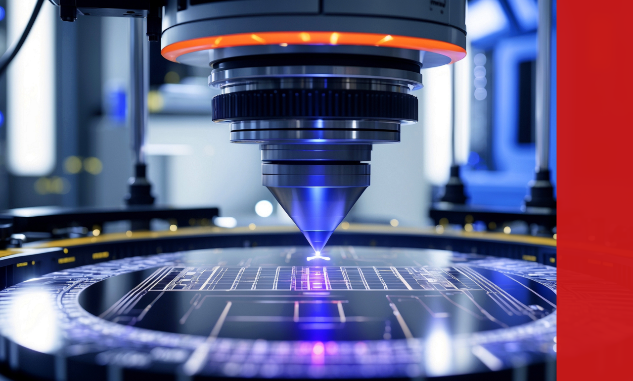
Dai Nippon Printing announced it has achieved 10nm line-pattern resolution on a nanoimprint lithography template, positioning the technology as suitable for logic semiconductors aligned with the “1.4nm generation.” While node names no longer directly correspond to physical dimensions, the announcement places NIL firmly in the conversation around leading-edge logic patterning.
Unlike conventional lithography, which relies on highly complex light-based exposure systems such as EUV, nanoimprint lithography transfers patterns through a mechanical imprinting process. A patterned template is pressed into a resist layer, effectively “stamping” circuit features onto the substrate. DNP describes NIL as a high-precision molding approach that bypasses some of the optical complexity inherent in advanced photolithography.
How DNP Reached 10nm Line Width
According to DNP, the move to 10nm lines was enabled through Self-Aligned Double Patterning, a technique where it increases pattern density by forming spacers around a primary pattern created using an electron-beam mask writer followed by deposition and etching steps.
DNP says it combined its long-standing photomask expertise with wafer manufacturing process technologies to develop the NIL template effectively bridging mask fabrication and wafer-level patterning know-how.
The energy-and-cost angle
Lithography remains one of the most energy-intensive and capital-heavy stages of semiconductor manufacturing. DNP claims that, in applicable use cases, NIL can reduce power consumption in the exposure step to about one-tenth of that required by ArF immersion and EUV processes.
This energy-saving claim aligns with broader industry interest in NIL as a potential cost- and power-efficient complement to EUV. By replacing large, complex exposure tools with a stamping-based approach, NIL has long been viewed as a way to lower both operational energy use and equipment costs.
Despite its promise, NIL has historically struggled to break into leading-edge manufacturing. Key challenges include defect and contamination control, as well as overlay accuracy when stacking multiple patterned layers at nanometer-scale precision. These issues have been well documented in industry and academic analysis, including coverage by IEEE Spectrum, which highlights alignment and defect management as major barriers to commercialization.
As a result, developments like DNP’s are best viewed not as a replacement for EUV, but as an expansion of the advanced patterning toolkit. NIL may ultimately find its role alongside EUV, serving specific layers or applications where its cost and energy advantages outweigh its limitations.
What comes next
DNP says it has already begun evaluation work with semiconductor manufacturer customers and is targeting mass production in 2027. The company has also set a commercial goal of growing NIL-related sales to ¥4 billion by FY2030, signaling confidence that the technology can move beyond the lab and into production flows.


