U.S. Invests $150M in xLight Free-Electron Laser as New EUV Lithography Source
Published: 12.8.2025
The United States is taking a bold step to reshape how the world’s most advanced chips are made.
Under a preliminary agreement, the U.S. government plans to provide up to $150 million in federal incentives to Palo Alto–based xLight, Inc. The funding will support the construction, build-out, and demonstration of a free-electron laser prototype in Albany, New York, designed as a new type of light source for extreme ultraviolet lithography. In return, the government would receive $150 million in equity in the company.
From policy vision to a concrete project in Albany
The incentives fall under the CHIPS and Science Act, through the Department of Commerce’s CHIPS R&D Office at NIST. While the agreement remains a non-binding Letter of Intent, it signals the government’s interest in making xLight’s FEL a core part of the U.S. lithography roadmap.
The FEL prototype will be deployed at the Albany NanoTech Complex, a core site for the planned National Semiconductor Technology Center. By placing the project in Albany, the U.S. is pairing a novel light source with one of the country’s most advanced R&D ecosystems for chipmaking.
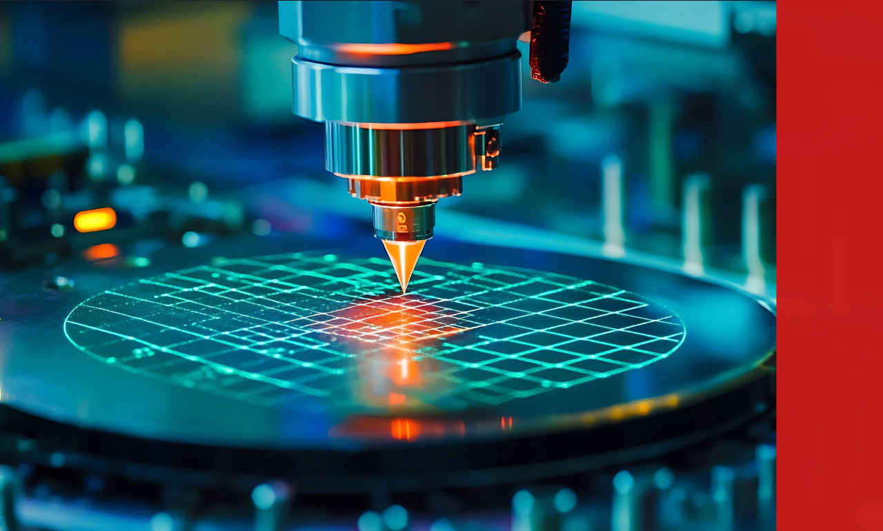
Modern chips rely on EUV lithography, which uses ultra-short-wavelength light to pattern silicon. Today, that light comes from laser-produced plasma which are power-intensive, costly, and difficult to scale.
xLight is pursuing a different model where its system uses a particle accelerator to speed electrons through a chain of magnets (undulators), generating EUV light in a more efficient way. Instead of housing the source inside each scanner, xLight proposes a centralized FEL facility that feeds light through optical transport lines to multiple EUV tools. If successful, one FEL could power several scanners at once, potentially boosting:
- Brightness and beam quality,
- Energy efficiency, and
- Throughput per scanner
The Albany project is expected to move through construction, commissioning, and demonstration over the next several years. During testing, the FEL will be paired with state-of-the-art EUV scanners and may also explore even shorter wavelengths, laying groundwork for future lithography generations.


