TSMC to Phase Out 6-Inch Wafer Production To Shift Toward Higher-Efficiency Fabs
Published: 8.14.2025
- TSMC phasing out 6-inch wafer production by 2027.
- Consolidation into more efficient 8-inch and 12-inch fabs.
- Strategic alignment with 30% YoY revenue growth and advanced manufacturing trends.
- Potential conversion of 6-inch fab site to advanced packaging hub.
- Implications for mature-node competitors and equipment suppliers.
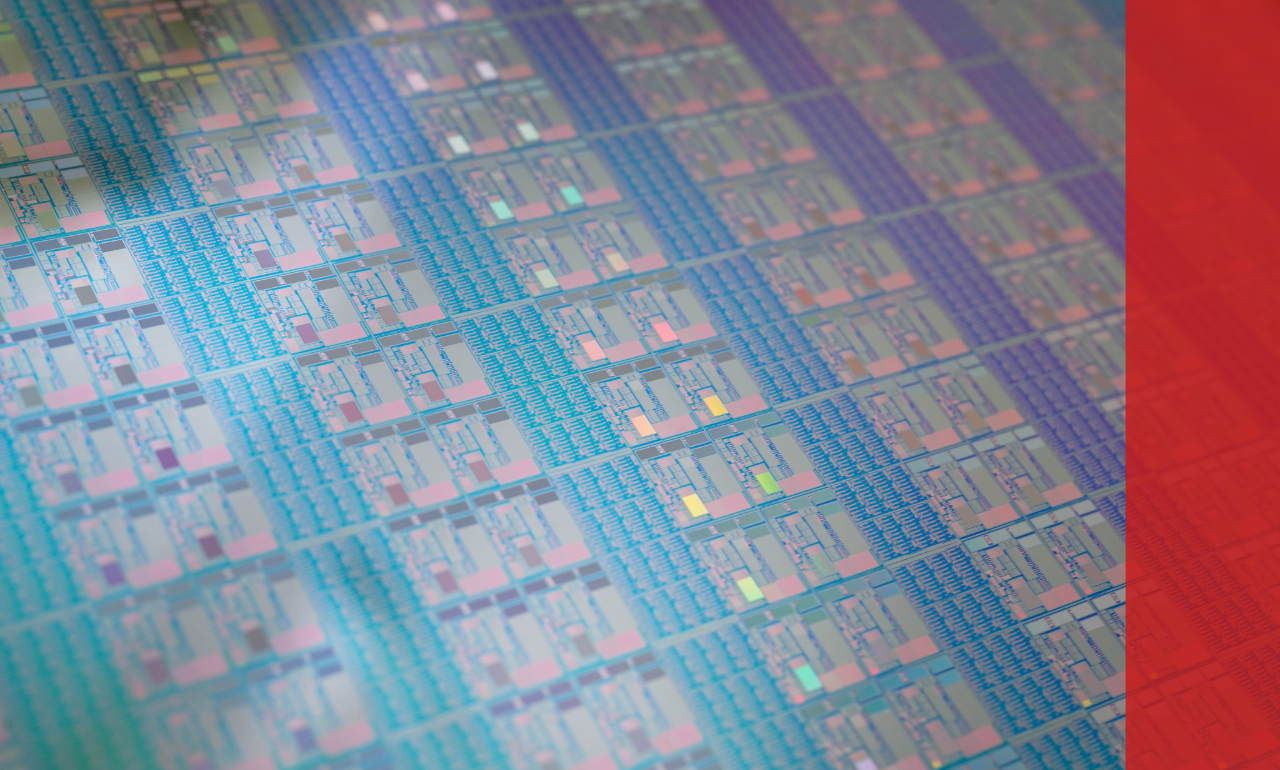
TSMC's Strategic Wafer Fab Transition
TSMC's Strategic Wafer Fab Transition
The strategic shift comes as the global semiconductor market is projected to reach US $728 billion in 2025, up 15.4% from last year, according to the World Semiconductor Trade Statistics (WSTS). With strong demand in logic, memory, and sensors, TSMC is positioning itself to capture more value in high-growth, high-efficiency manufacturing segments.
The decision will see TSMC wind down operations at its 6-inch line—also known as Fab 2—by 2027. Historically, this mature-node facility has supported production for niche analog ICs, MEMS, sensors, and certain power management chips. By shifting customers to larger wafer sizes, TSMC aims to achieve lower cost per die, higher yield density, and better equipment utilization.
In a public statement, TSMC indicated the phase-out is part of a “planned and orderly transition” with minimal disruption expected for customers. The company has already begun coordinating with clients to migrate designs and production to compatible 8-inch processes.
Future Prospects and Industry Implications
Industry analysts note that the 6-inch fab site may not be left idle. Reports suggest TSMC is evaluating converting the facility into an advanced IC packaging and assembly hub—a move that would bolster its capabilities in AI-oriented chiplet and 3D-IC technologies.
While the 6-inch market remains relevant for certain low-volume and legacy applications, industry observers see the exit as a signal for other foundries and suppliers to adjust capacity planning. Competing mature-node fabs in the U.S., China, and India may benefit from customers seeking to maintain 6-inch production capacity outside of TSMC’s ecosystem.
For suppliers of specialized 6-inch equipment and materials, the change could prompt a pivot toward supporting 8-inch or specialty wafer markets, such as gallium nitride (GaN) or silicon carbide (SiC).


